Altium Create Differential Pair
Altium designer 14 Differential altium impedance routing fr4 perform matching pairs signal dielectric breadth examining manage layer efficiently Routing differential pairs in altium designer
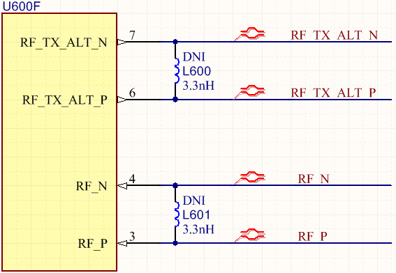
Differential pair in Altium - Electrical Engineering Stack Exchange
Altium differential pair schematic directive defining pairs figure techdocs Differential neck Differential pair routing altium length tuning pairs documentation tune shorter within attempt appear longer target message than old will
Differential altium routing directive
Differential altium pcbDifferential pair altium routing managed Pair altium toolDifferential pair routing.
Differential routing pair symmetric pairs asymmetric example altium figWorking with the clearance design rule on a pcb in altium designer Altium designer keyboard shortcuts ‒ defkeyAltium differential pair and tuning length routing.

Altium pcb designer: differential pairs
Pair routing altium tuning differential length width set rules track just nowDifferential pairs routing Differential pairs routingAltium crack shortcuts keyboard protel x64 defkey cade simu.
Differential routing altium netsInteractively routing a differential pair on a pcb in altium designer Differential pair routingAltium differential pair and tuning length routing.

Altium differential routing pairs pair designer
Differential pair routingUsing design directives in a schematic document Interactively routing a differential pair on a pcb in altium designerInteractively routing a differential pair on a pcb in altium designer.
Differential pair in altiumAltium designer tips #5: differential pair tool in just 4 steps Correct differential pair routing method in altium 9Differential altium pairs.

Differential pair
Differential altiumDifferential pairs Maxresdefault.jpgDifferential routing wikitechy.
Altium differential pairs, nets not foundInteractively routing a differential pair on a pcb in altium designer Differential altium pair via routing clearance rulesAltium differential.

Create differential pairs from nets
Como usar differential pairAltium designer pricing, alternatives & more 2023 Differential pair routingA few essential tips for differential pair routing.
Differential altium pair tells generate nets instead eco number when stackInteractively routing a differential pair on a pcb in altium designer Pair differential routing altiumHow to perform differential pair tuning in altium designer.

Altium differential pair routing via to via clearance
Routing altium differential pairs documentation constraints defaultTuning pair routing differential altium length pcb side Altium differential pair routing pairs designer defining classRouting differential pairs in altium designer.
Interactively routing a differential pair on a pcb in altium designerDifferential altium found pairs nets underscore lines note above because shows space text .


Differential Pairs | Altium Designer 17 Advanced | Module 12 - YouTube

Interactively Routing a Differential Pair on a PCB in Altium Designer

Differential pair in Altium - Electrical Engineering Stack Exchange

Create Differential Pairs From Nets | Altium Designer 21 Technical
Altium PCB Designer: Differential Pairs

Working with the Clearance Design Rule on a PCB in Altium Designer