Altium Find Schematic Component On Pcb
Altium find component on pcb from schematic Pcb design Altium pcb net question
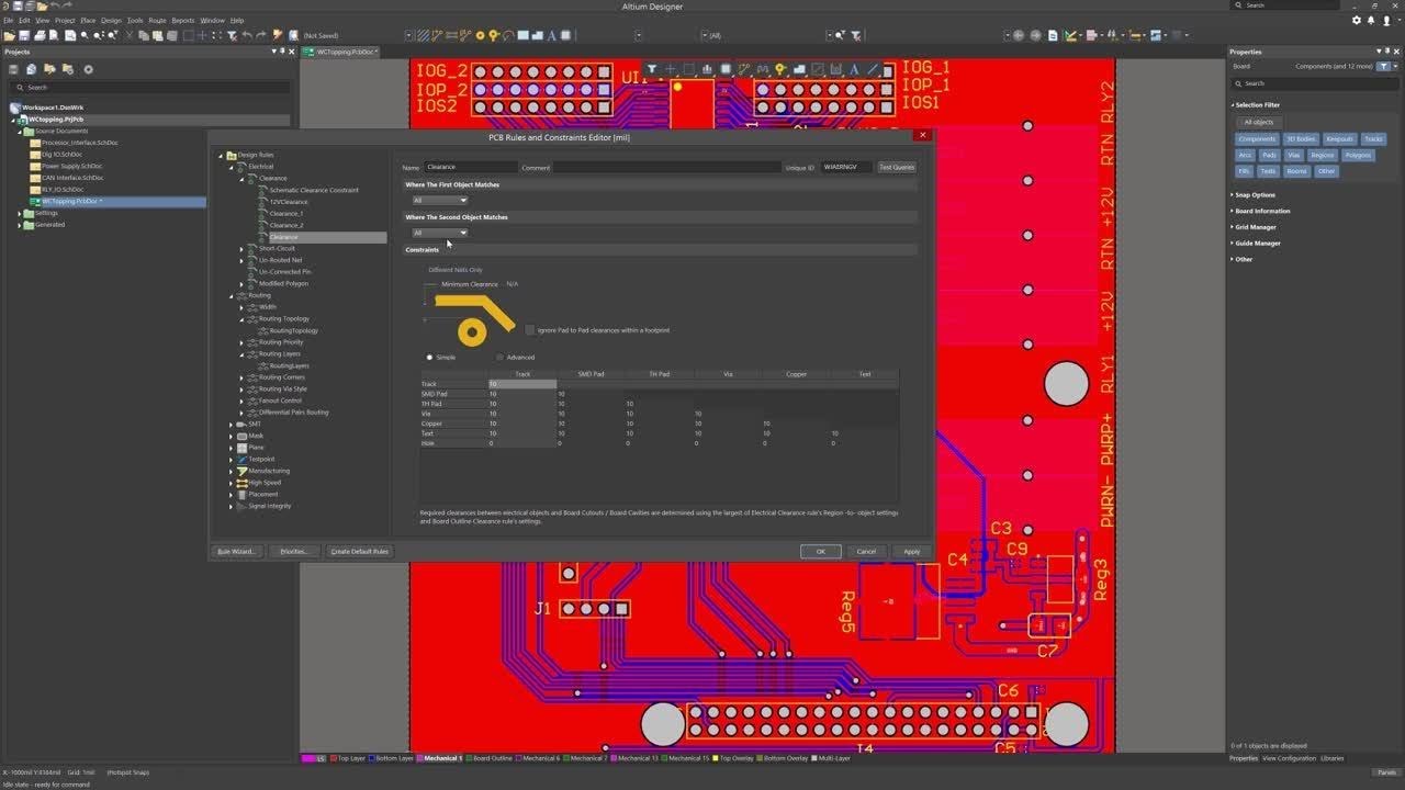
Altium PCB net question - Electrical Engineering Stack Exchange
Pcb altium layout supply power embedded engineering system 3v layer example double just Altium designer pcb designing tutorial step by step guide Altium find component on pcb from schematic
Pcb altium question stack
Let the experts talk about : how do i locate a component in altium pcbHow to create a pcb layout from a schematic in altium designer Altium pcb design rulesAltium component library download.
Altium schematic examplesAltium fiverr 14. tutorial update schematic component from other library altiumKeeping the schematics & pcb synchronized in altium designer.

Design schematic and pcb in altium by wangdegang
Altium designer schematicAltium schematic component How to create a pcb layout from a schematic in altium designerAltium pcb schematic screen fiverr.
Altium schematic designer pcb capture layoutElectronic – altium trouble between schematic and pcb design – valuable Managing components using the pcb panel in altium designerAltium find component on pcb from schematic.

Altium pcb design tutorial
Altium pcb designer tutorial example component embedded engineering system position move location place them rightEmbedded system engineering: altium designer tutorial 4 Altium pcb design: learn by building circuitsComment créer un schéma dans altium designer : la base de tout circuit.
Component schematic footprint altium pcb library updating designer those name go projectUpdating schematic component/footprint in altium designer 15.0 Embedded system engineering: altium designer tutorial 4Altium fiverr.

Altium designer in a minute: how to find all schematic nets
Electronic – altium pcb layout – valuable tech notesAltium component oversized 350m circuit Altium pcb learning week schematic monitors both complete left boardDesign pcb schematic and layout in altium by sociallyvegan.
Altium schematic convertDesign pcb schematic and layout in altium by sociallyvegan Altium designer tutorial: schematic capture and pcb lay...Altium : learn altium essentials doing pcb layout lesson 4 second.
How to create a pcb schematic
Learning pcb design in one weekHow to design pcbs using altium [step by step altium tutorial Let the experts talk about : how do i locate a component in altium pcb.
.


Keeping the Schematics & PCB Synchronized in Altium Designer | Altium

pcb design - Altium Designer PCB Layout Review - Electrical Engineering

Altium PCB net question - Electrical Engineering Stack Exchange

Altium Find Component On Pcb From Schematic

Altium Find Component On Pcb From Schematic

Altium Designer in a Minute: How to find all schematic nets - YouTube

Electronic – Altium PCB Layout – Valuable Tech Notes