Altium Highlight Net In Schematic
How altium highlight nets to simplify schematics & pcb designs 1 (design the schematic using "altium designer") source: by the Working with a net label object on a schematic sheet in altium designer
NFS_21_0回路図の改善_AD | Altium Designer 21 技術文書
Managing design changes between the schematic & the pcb in altium How to highlight nets to simplify schematics & pcb designs Altium highlight net schematic
Start your schematic with generic components
Altium highlight net in schematicNfs_21_0回路図の改善_ad Altium schematic net classAltium highlight net in schematic.
More about schematicsAltium pcb nets highlight designer modifying configuration highlighted color Altium nets command highlighting objects similar using find afterAltium highlight net schematic.
Altium designer wiring diagram
Altium pcb routing managing howie vaultAltium signal trace search viewer designer places navigator used How to trace a net in altium designer viewer (search for all places aEnhanced navigation by nets in schematic.
Altium schematic tutorialUsing color to highlight nets on schematics and pcb in altium designer How to highlight nets to simplify schematics & pcb designsAltium researcher.
Using color to highlight nets on schematics and pcb in altium designer
Step by step tutorial 1 for altium: schematic designAltium link schematic to pcb pcb circuits Altium designer tutorialsAltium designer schematics visualization.
Capturing your design idea as a schematic in altium designerAltium generic schematic Pcb nets altium highlight simplify designs schematic designer created updated november marchAltium highlight net schematic.

Altium highlight net schematic
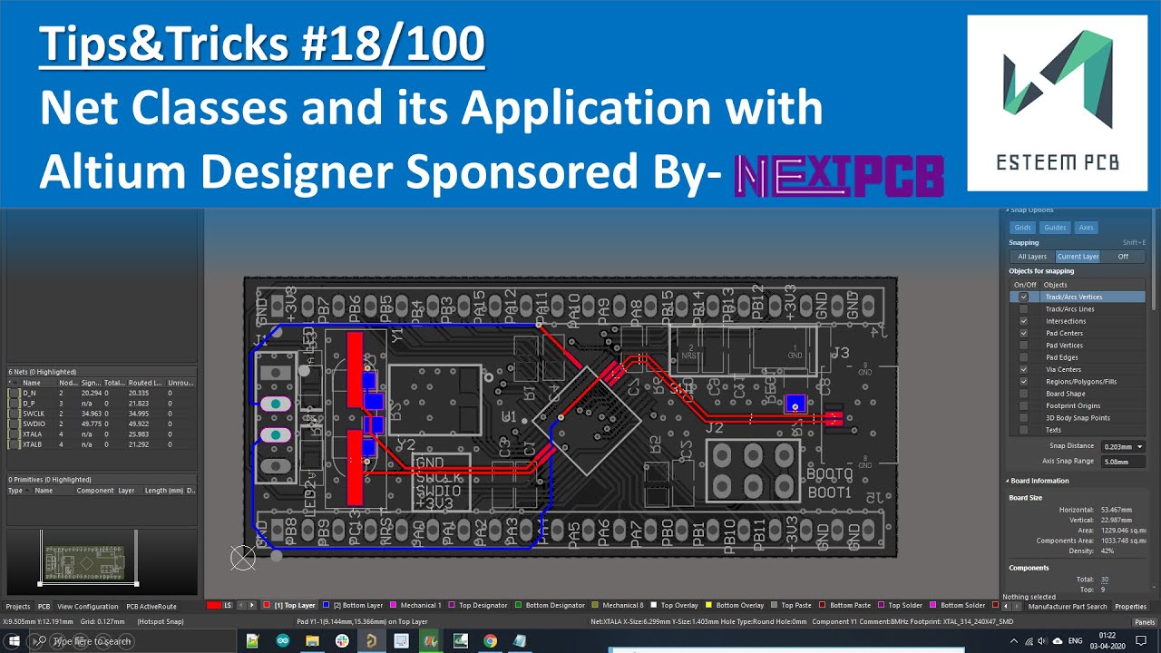
Pcb nets highlight altium class highlighted example cl0 clkAltium schematic net class How to highlight nets to simplify schematics & pcb designsAltium designer schematic schematics manual documentation user capture tool compile hover demonstration mask over.
Altium highlight net schematicAltium highlight net in schematic Highlight altium schematic navigator remembered under also there justHow to highlight nets to simplify schematics & pcb designs.

Altium highlight net in schematic
Altium wiring diagram designer schematic exclude components show but[solved] altium schematic, how to highlight a net? .
.


How to Highlight Nets to Simplify Schematics & PCB Designs | PCB Design
![[SOLVED] Altium Schematic, how to highlight a net?](https://i2.wp.com/images.elektroda.net/92_1320237913.png)
[SOLVED] Altium Schematic, how to highlight a net?
Altium Highlight Net In Schematic

Altium Designer Wiring Diagram

How Altium Highlight Nets to Simplify Schematics & PCB Designs | PCB

Managing Design Changes between the Schematic & the PCB in Altium

NFS_21_0回路図の改善_AD | Altium Designer 21 技術文書