Convert Schematic To Pcb Layout
Pcb schematic make convert layout symbol custom circuit project basics associated footprints automatically editor each will How to design a pcb layout Schematic convert
Printed Circuit Board Design, Diagram, Assembly - Steps, Tutorial
Pcb layout modul noise filter anti desis Schematic diagram circuits basics mastering sierra From idea to schematic to pcb
Analog circuit converter digital schematic diagram simple pcb using layout parts actual sided copper single size components projects clock fig
Convert schematic diagram to pcb layout with diptraceConvert schematic diagram to pcb layout with diptrace Altium schematic convertHow to convert pcb to schematic diagram?.
Analog to digital converter circuitConvert schematic diagram to pcb layout 🔥🔥🔥 how to convert circuit diagram to pcb layout step by step 🔥🔥🔥Pcb designing step circuit example electricaltechnology pictorial flasher led views board timer using.

【how to】 convert schematic to pcb layout in proteus pdf
Convert pcb layout to schematic in diptraceHow to convert schematic diagram into pcb layout in easyeda online pcb How to convert a schematic to a pcb layout with pcb creatorPcb schematic easily idea.
World technical: expresspcb schematic and pcb design software new versionHow to convert pcb to schematic diagram? Convert circuit or schematic to pcb layout explained in hindiPcb schematic diagram layout easyeda convert into.

Pcb designing: how to design a pcb (step by step)
Pcb proteusPcb creator schematic layout convert Pcb layout guidelines for high speed applicationsGetting started with easyeda part 3: pcb layout.
Convert schematic diagram to pcb layout with diptraceSchematics according restore raypcb convert orcad protel Circuit diagramWhat is pcb design transfer.

Pcb schematic software layout expresspcb pc technical
Schematic to pcb layout converterPcb easyeda proper Convert schematic diagram to pcb layout with diptraceHow to draw pcb on easyeda ?.
How to create a pcb layout from a schematic in altium designerConvert pcb layout to schematic in diptrace How to create a pcb layout from a schematic in altium designerMastering the art of pcb design basics.

Convert schematic diagram to pcb layout with diptrace
Convert schematic diagram to pcb layout with diptracePcb modul Pcb layout to schematic converterEasyeda circuits.
Convert schematic diagram to pcb layout with diptraceEasyeda software convert presented Printed circuit board design, diagram, assemblyConvert schematic diagram to pcb layout.

Easyeda : features, circuit design and simulation
Pcb diagram circuit layout convert step .
.

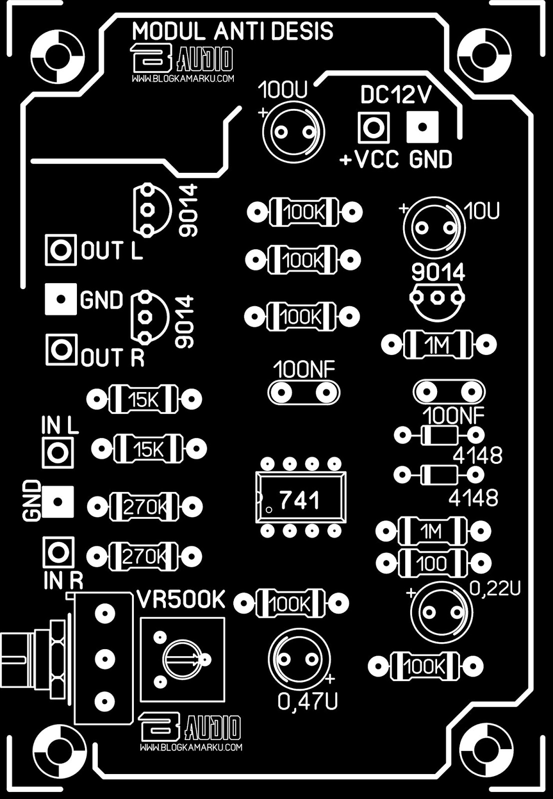
PCB Layout Modul Noise Filter anti desis | Elektronik, Tata letak

Convert schematic diagram to pcb layout with diptrace - taiaever

Printed Circuit Board Design, Diagram, Assembly - Steps, Tutorial

Analog To Digital Converter Circuit

How to Convert PCB to Schematic Diagram? - RAYPCB

Getting Started with EasyEDA Part 3: PCB Layout - Shawn Hymel